|
مجال
التميز
|
تميز دراسي وبحثي
|
|
البحوث المنشورة
|
|
|
البحث (1):
|
|
|
عنوان البحث:
|
Initial Stages in the Formation of Cu2ZnSn(S,Se)4
Nanoparticles
|
|
رابط إلى البحث:
|
click
here
|
|
تاريخ النشر:
|
21 OCT 2013
|
|
موجز عن البحث:
|
In the beginning: Intermediate species generated
in the synthesis of Cu2ZnSn(S,Se)4 nanoparticles (see figure) in oleylamine
have been identified. The solvent plays a central role in the reaction
mechanism, determining the composition of the nanostructures.
|
|
البحث (2):
|
|
|
عنوان البحث:
|
Crystal Structure
and Defects Visualization of Cu2ZnSnS4 Nanoparticles Employing
Transmission Electron Microscopy and Electron Diffraction
|
|
رابط إلى البحث:
|
Click
here
|
|
تاريخ النشر:
|
November 2015
|
|
موجز عن البحث:
|
A detailed analysis of the structure of
Cu2ZnSnS4 (CZTS) nanocrystals synthesized by hot-injection in the
presence of oleylamine is provided employing high resolution TEM, selected
area electron diffraction (SAED) and convergent beam electron diffraction
(CBED). The nanostructures were investigated as-grown and after vacuum
thermal treatment at 550 °C. As-grown materials consisted of
polycrystalline particles with an average size of 7 ± 3 nm,
which grow an average size of 53 ± 13 nm after the vacuum
annealing step. This thermal treatment allows investigating the initial
stages of high quality film growth required in photovoltaic devices. Sets of
SAED and CBED patterns, where individual crystals after annealing were viewed
down different prominent zone axes, enabled us to reveal the presence of weak
reflections due to cation ordering, and confirm a tetragonal unit cell
consistent with either the kesterite or stannite structure. We demonstrate
how these approaches enable to distinguish CZTS from secondary phases such as
ZnS. Structure defects of partially annealed CZTS crystals were also
investigated using bright and dark field images taken in 2-beam diffraction
conditions as well as by high resolution lattice imaging. The material exhibited
dislocations, along with lamellar twins and stacking faults characterized by
local hexagonal structure on {112} planes. High resolution TEM images showed
preferential growth on {112} planes during vacuum annealing, which is
consistent with X-ray diffraction patterns. These studies provide key
information on nanoscale crystal defects which may have important consequence
on the performance of CZTS photovoltaic devices.
|
|
المؤتمرات العلمية:
|
|
|
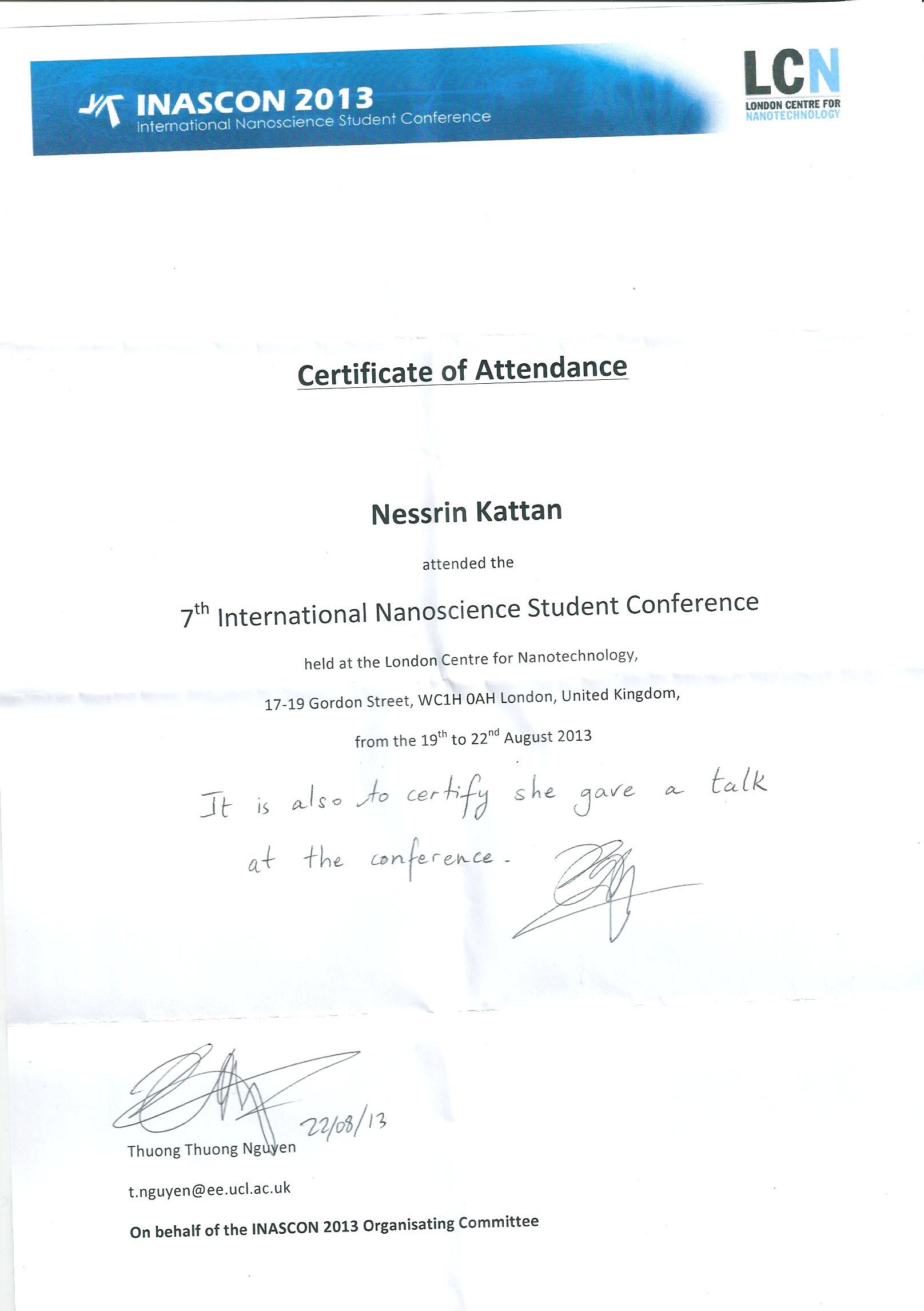
المؤتمر (1):
|
|
|
عنوان المؤتمر:
|
Great Western Photoelectrochemistry Meeting
|
|
تاريخ الإنعقاد:
|
09 Jun 2014
|
|
مكان
الإنعقاد:
|
Bath, UK
|
|
طبيعة المشاركة:
|
Poster presentation
|
|
عنوان المشاركة:
|
Cu2ZnSnS4: low cost
material for thin film solar cells
|
|
ملخص المشاركة:
|
Cu2ZnSnS4
(CZTS), being related to the highly successful Cu(In,Ga)(S,Se)2,
and CuInS2 materials, is a promising candidate for thin film
photovoltaic devices. It has the advantage that it contains abundant and low
cost elements, and therefore has cost-reduction potential for commercial
systems. In this work, CZTS nanocrystals have fabricated into thin films
using spray technique. The films were annealed at different atmosphere
conditions, vacuum, Argon, Nitrogen, sulfur and selenium. The results films
were characterized using scanning electron microscope (SEM) to investigate
the morphology and the nanocrystal growth. The photoresponse of the CZTS
nanocrystal films was evaluated using photoelectrochemical methods in aqueous
electrolytes. Photoelectrochemical characterization revealed a p-type
photoresponse when the films were illuminated in an aqueous Eu3+ redox
electrolyte. The best photocurrent result is achieved from stoichiometric
CZTS by anneal the film in vacuum achieving IPCE of 8.2%.
|
|
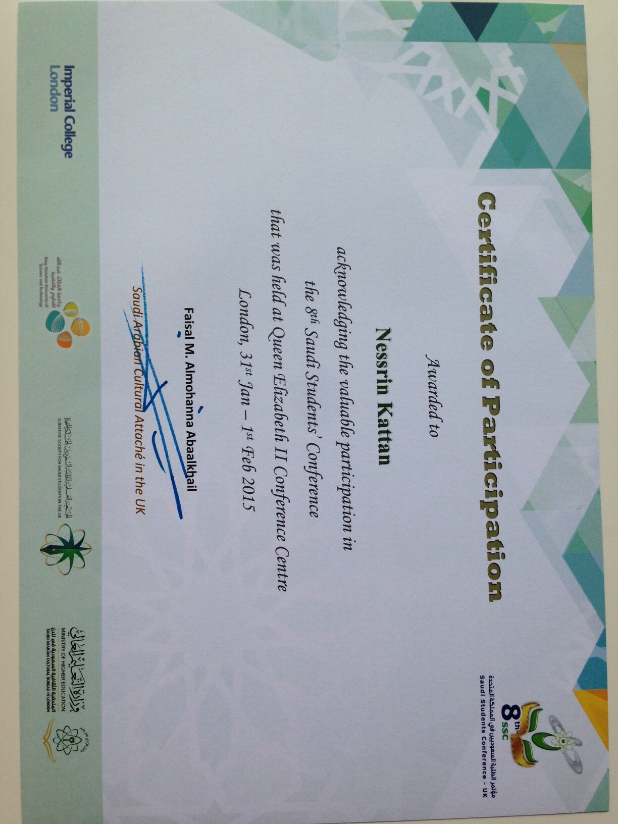
المؤتمر (2):
|
|
|
عنوان المؤتمر:
|
The 8th Saudi Student Conference
|
|
تاريخ الإنعقاد:
|
33 Jan to
01 Feb 2015
|
|
مكان
الإنعقاد:
|
London,
UK
|
|
طبيعة المشاركة:
|
Poster presentation
|
|
عنوان المشاركة:
|
Photovoltaic
technology based on earth abundant materials
|
|
ملخص المشاركة:
|
Quaternary semiconductor Cu2ZnSnS4
(CZTS) is a remarkable alternative absorber material for the conventional
technologies. CZTS has the advantage of containing only earth abundant and
non-toxic elements. It has nearly ideal direct bandgap of 1.4-1.6eV and high
optical absorption coefficient of ~104cm-1. In this
work, transmission electron microscopy (TEM) was applied to confirm the pure
phase of CZTS by investigating the crystal structure of as-prepared material,
before and after annealing. The material was analysed using selected area
(SAED) and convergent beam electron diffraction (CBED) techniques. A
polycrystalline material was formed in the pre-annealing stage. SAED and CBED
patterns from the annealed material showed tetragonal unit cell consistent
with a Kesterite or stannite phase. The growth of CZTS nanoparticles is also
investigated. We introduced a new method using hydrogen annealing atmosphere
to improve the growth of the nanoparticles from initial size of ~10 nm up to
micron crystals size
|
|
المؤتمر (3):
|
|
|
عنوان المؤتمر:
|
Electron
Microscopy and Analysis Group (EMAG) Conference 2013
|
|
تاريخ الإنعقاد:
|
3-6 September 2013
|
|
مكان
الإنعقاد:
|
University of York, UK
|
|
طبيعة المشاركة:
|
Poster presentation
|
|
عنوان المشاركة:
|
Crystal
structure and defect analysis of solution processed Cu2ZnSnS4
using transmission electron microscope
|
|
ملخص المشاركة:
|
Si, CdTe, and CIGS are the most interesting
absorber material used for thin film solar cells applications. These systems
have achieved high efficiency and reached the commercialized stage. However,
they have many drawbacks due to their scarcity and toxicity. In the last two
decades, intensive studies curried out on Cu2ZnSnS4
(CZTS) as an ideal alternative absorber layer for photovoltaic devices due to
their low cost, abundance and safety to the environment. In this work, the
crystal structure of as-synthetic material and after annealing was analysed
by selected area (SAED) and convergent beam (CBED) electron diffraction
techniques. TEM is an accurate technique to identify the actual phase of the
material since other methods such as X-ray diffraction and Raman spectroscope
are controversial. SAED and CBED patterns are collected from different
directions of CZTS nanocrystals and analysed to investigate CZTS crystal
structure. Diffraction patterns of crystalline material confirmed CZTS phase
showing superlattice reflections extended along [001] c-axis which reveal to
tetragonal unit cell. Furthermore, Superlattice domains observed in the
bright field and dark field TEM images that extended parallel with the
tetragonal c-axis
|
|
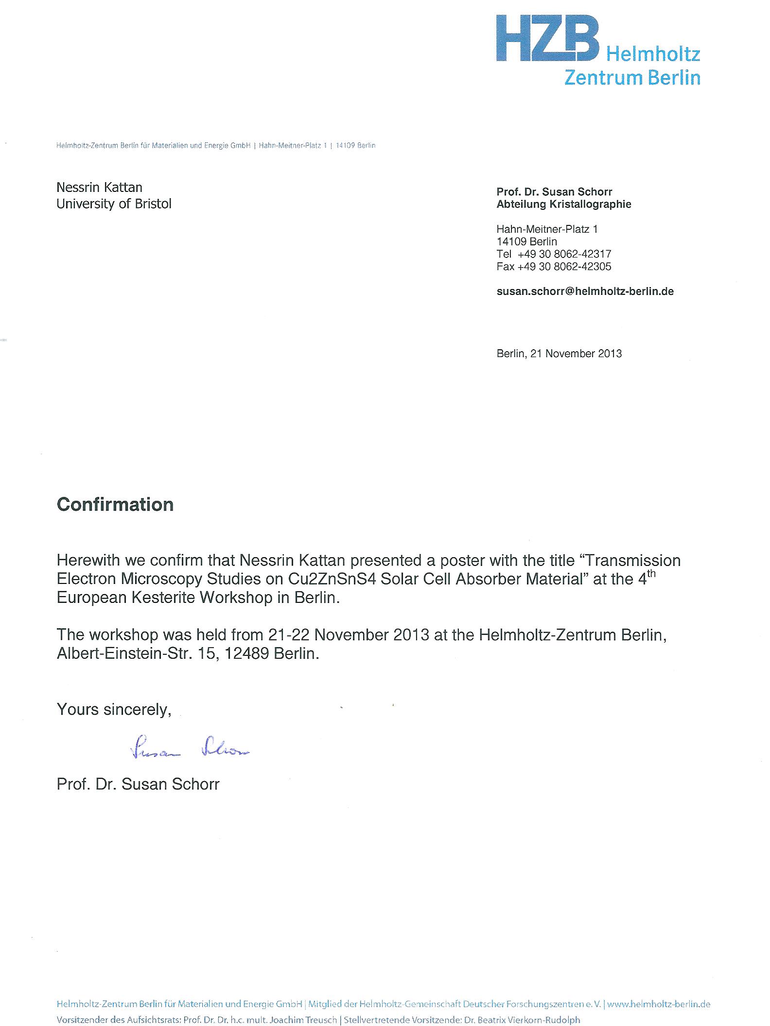
المؤتمر (4):
|
|
|
عنوان المؤتمر:
|
The 4th European Kesterite Workshop
|
|
تاريخ الإنعقاد:
|
21/11/2013
|
|
مكان
الإنعقاد:
|
Helmholtz-Zentrum
Berlin, Germany
|
|
طبيعة المشاركة:
|
Poster presentation
|
|
عنوان المشاركة:
|
Transmission
Electron Microscopy Studies on Cu2ZnSnS4 Solar Cell
Absorber Material
|
|
ملخص المشاركة:
|
Copper zinc tin sulphide (CZTS) has been
attracted a lot of attention over the last two decades. Its importance lies
in their availability and safety to the environment in additional to its low
cost. The defect structure of CZTS was investigated by bright and dark field
images techniques on transmission electron microscope taken in 2-beam
diffraction conditions. In the post annealed stage, the material showed a low
density of lamellar twins and dislocations at {112} planes. The crystal
structure of these defects was investigated using high resolution (TEM)
lattice images showed changing of stacking sequence from cubic basic
structure to hexagonal (wurtzite) structure occurred at twining boundaries
|
|
المؤتمر (5):
|
|
|
عنوان المؤتمر:
|
European Materials Research Society
|
|
تاريخ الإنعقاد:
|
11-15/05/2015
|
|
مكان
الإنعقاد:
|
Lille, France
|
|
طبيعة المشاركة:
|
Poster presentation
|
|
عنوان المشاركة:
|
Structure,
Growth and Defects in CZTS Films Processed from Nanocrystals
|
|
ملخص المشاركة:
|
Transmission
electron microscopy (TEM) has been used to investigate the crystal structure
and defects of both as-prepared and post annealed CZTS nanocrystals that were
produced by the hot injection technique. CZTS annealing proceeded in vacuum.
Selected area electron diffraction (SAED) and convergent beam electron
diffraction (CBED) techniques showed the as-prepared nanoparticles to have a
cubic structure with some evidence of tetragonal structure for larger
nanoparticles. This suggests the presence of two polymorphs in the
as-prepared material. The post-annealed CZTS showed more crystalline
particles that result of producing a pure phase of tetragonal crystal
structure consistent with kesterite phase. The defects were investigated
using bright field (BF) and dark field (DF) techniques on TEM, and showed the
formation of lamellar twins in annealed CZTS nanocrystals with the formation
of a local hexagonal structure at twin boundaries.
Another
crucial issue that has been investigated in this work is the growth of CZTS
nanocrystals during annealing. We studied the effect of different annealing
conditions on the growth of CZTS nanocrystals such as (H2/N2, N2, Ar, S, Se,
SnS, Na2S, and vacuum). Annealing in a hydrogen atmosphere achieved the best
grain growth, with sizes reaching more than a micron from initially ~10 nm
particles. The presence of H2 was also found to minimize the carbon content
of the resulting films.
|
|
الجوائز التكريم:
|
|
|
مسمى الجائزة:
|
1st
Poster Prize
|
|
الجهة المانحة:
|
the
Great Western Photo-Electrochemistry Meeting GWPEM 2014
|
|
تاريخ الجائزة:
|
9th June 2014
|
|
مجال التكريم:
|
Cu2ZnSnS4:
Low Cost Material for Thin Film Solar Cells
|


